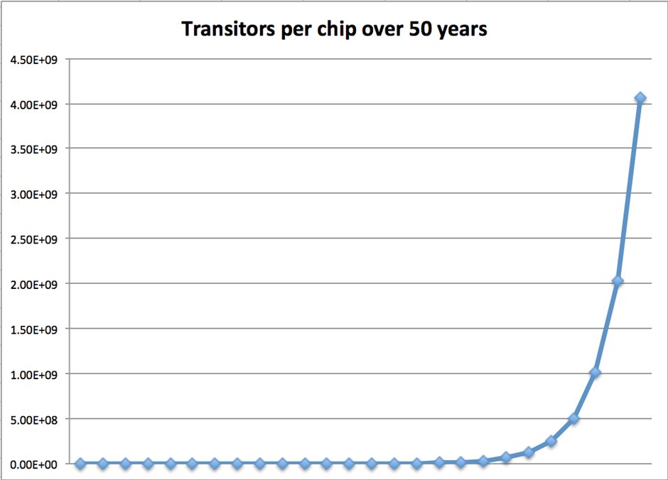
April 19 marks the 50th anniversary of Moore’s law. This is not just a very significant anniversary for technology, but for all of mankind.
Here is why. We have never before seen such explosive innovation on such a massive and sustained scale.
Let me break it down. Gordon Moore formulated his vision about semiconductor complexity explosion in 1965. Originally, he predicted a doubling of the number of components on a chip every year. Later he revised it to occur every two years.
What does this mean when we compare 1965 to 2015?
It means 225 = 33,554,432
In other words, we have witnessed a 33 million-fold explosion in terms of transistors in an integrated circuit (IC). Today, the largest ICs count transistors in the billions!
For example, Intel’s latest 15-core Xeon Ivy Bridge-EX has over 4 billion transistors.
In no other field of human undertaking have we seen such a long stretch of exponential growth. It is absolutely astounding.
Furthermore, in no other field can you predict that the complexity and its associated application potential will double every two years!
However, we are standing at an inflection point. Moore’s law, let me call it Moore’s law 1.0, will most likely reach its end within a decade. The main premise of Moore’s law is driven by how many components can be packed on a chip. In Moore’s law 1.0 we dealt primarily with a two-dimensional area – the width and length of silicon structure to be manufactured. The latest process size is 14nm. The next-generation process size will be 10nm and 11nm, respectively.
Why are even smaller structure sizes a problem, and why can we not go significantly into the sub-10nm space?
It comes down to the size of the silicon atom and the associated silicon lattice. The lattice parameter alpha for silicon is only about 543 picometers. This means we are dealing with only about 18 layers of Si for a thickness of a 10nm wide lattice. However, with modern transistors things are even smaller as we are now using FinFET technology. The fin width in a 14nm process transistor is actually only 8nm! This is equivalent to about 15 layers of silicon lattice.
At the sub-10nm level, electromigration, and process variations in manufacturing, amongst other effects, will be so large that the end of conventional silicon chip manufacturing at high yields and chip longevity might be reached.
However, we have a way out of this predicament. The solution is to build up.
If we cannot make it 2D anymore, let’s make it 3D. Think about Manhattan, in New York City. When 2D space gets tight you build up into 3D space. The same thing is occurring in semiconductor manufacturing.
Indeed Samsung recently announced a new type of Flash memory: V NAND Flash memory that stacks 32 component layers (up from 24) on top of each other, creating much more capacity per chip than has ever been seen before.
The geometric regularity of memory elements lend themselves perfectly to this kind of application. But we need more than densely stacked memories. We need CPU cores, GPU cores, controllers, bridges, and so on.
From a manufacturing perspective, Moore’s law will go into the Z-dimension to achieve its gains. However, from a computing perspective, the new paradigm will be massive parallelism. The only way to increase compute power is to leverage parallelism because we cannot increase clock frequency much further. The end of conventional silicon manufacturing will force us to go this direction. Subsequently, software development will need to adapt to take advantage of ultra-multi core computing. Ultra-multi core means initially hundreds, but soon thousands of cores and more.
Conventional multi-threading won’t be enough and parallelism will no longer be for special applications or subsets of application. It will be the heart of compute speed, and any application with a need for high-speed computing will need to adapt to it.
Intel and ARM-based chips have been multi-core for years. In fact, you can hardly buy a high-volume, single-core CPU any more.
But those multi-cores all live in two dimensions. In the 3D world we will see a core explosion.
Today you can buy an off-the-shelf 15-core, high-end Intel Xeon chip. Imagine if it was fabricated in 32 layers and you now suddenly have 480 cores on the chip! This is a different beast altogether and will change hardware and software development dramatically.
Moore’s law 2.0 will be about component layers and the associated number of cores!
Axel Scherer
Chief Parallelism Guy
