The Integrity and Data Encryption (IDE) was published in PCIe (Peripheral Component Interconnect Express) version 6.0, and it was created as a tool to protect the communication between the different devices of the PCIe topology root complex (RC), switch (SW), and endpoint (EP). The IDE layer is a new layer that was inserted between the transection layer and data link layer with the goal of protecting against threats from physical attacks on the link. The IDE will use a cryptography mechanism to encrypt all data sent for both sides.

Figure 1 - Layers of PCIe Device
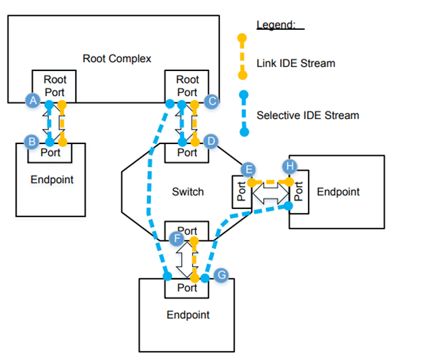
The IDE feature has two types of streams: the link IDE stream and the selective IDE stream. The link stream, in yellow, is a security channel in the link, and the selective stream, in blue, is a security channel between devices, not necessarily in the same link.

Figure 2 - IDE Secures TLPs Between Ports
The IDE has an internal finite state machine (FSM) with two states: the insecure; and the secure state. The stream will be insecure until it is configured and enabled. The PCIe gen 6.0 has a setup defined. However, the IDE has flexibility to other setups. In this blog, we will focus on the PCIe one. To configure the stream, first is requested to create the stream and configure the set of keys and INIV. After the configuration of the stream, it can be enabled. The IDE FSM will move to secure and stay in this state if no errors are detected or the stream is deactivated. During the secure state, is it possible to alternate between two sets of keys, warning, when the set of keys is changed, that the older set is invalid and must be reconfigured. The stream is enabled by setting the bit 0 of the link IDE stream control register in a link stream and the bit 0 of the selective IDE stream control register to selective stream.

Figure 3 - IDE State Machine
The space register of the IDE cap is shown in figure 4. As you can see, the IDE cap allows 8 link streams and 256 selective streams. All functionalities supported by the IDE CAP are defined in the IDE capabilities register.

Figure 4 - IDE extended capability structure
In this memory map, is it possible to see other useful registers, for example the IDE address association register, that define memory spaces that, if you want to be accessed, all packages must be encrypted.
You may question yourself: if the data TLP is encrypted, how to identify the TLP? And the answer is by the prefix. The prefix that the format and type is 0x92, and this prefix will inform the current Stream (Stream ID filed) and the set of key (K bit).

Figure 5 - IDE TLP Prefix
More Information
- For more info on how Cadence PCIe Verification IP and TripleCheck VIP enable users to confidently verify IDE, see our webpages on VIP for PCI Express, VIP for Compute Express Link, and TripleCheck for PCI Express
- For more information on PCIe in general, and on the various PCI standards, see the PCI-SIG website.