The ever-increasing innovations in artificial intelligence (AI) are revolutionizing the future, be it in self-driving cars, manufacturing, finance, education, and healthcare. AI, in simple terms means that a computer can perform the tasks which would typically need human intelligence. It is achieved by algorithms and models that enable computers to analyze and learn from huge amounts of data, reach the findings, and solve problems. This can be described in correct technical terms as training and inference. Training needs lots of compute and memory. Memory has been trailing compared to compute and it has become a bottleneck.
High-bandwidth memory (HBM) can help unclog the above-mentioned obstructions.
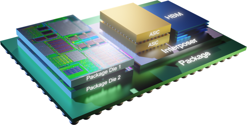
HBM is a dynamic random access memory (DRAM) standard defined by the Joint Electron Device Engineering Council (JEDEC), having a 3D-stacked memory architecture that reduces power consumption and has a small form factor.
Image may be NSFW.
Clik here to view.
HBM is close to the processor memory, and it is placed along with the SoC in the same package using an interposer. Unlike traditional memories, where they are scattered, HBM is vertically stacked and can be a lookalike of a multi-story data building as described in the image above. Various factors that make HBMs best for the AI industry are:
Bandwidth:
Vertical stack is a unique architecture that helps faster communication with processors or AI hardware accelerators and achieves bandwidth in terms of ~TB/s. This also enables tight memory integration in rising customer silicon designs to cater to AI needs. Even with a similar ~Gbps per pin speed, like other DRAMs, because of HBM’s Wide IO design, massive bandwidth can be achieved. Internally, the HBM device has multiple channels, which allows many data locations access at any moment of time. Further, it has semi-independent pseudo channels (PC) that help to read/ write from each PC simultaneously.
Area:
HBM has a smaller form factor by stacking memory chips vertically and that results in a high-density device.
Power:
Another common issue for AI hardware is the ever-growing demand for more processing power. HBM has features like data bus inversion (DBI), which reduces the number of signal toggles during data transfers. Even the latest HBM3 JEDEC standard (JESD238) released in Jan 2022 has included low-swing (0.4V) signaling to improve energy efficiency.
Apart from the above factors, HBM has high platform-level reliability, availability, and serviceability (RAS) by having on-die error correcting code (ECC), address, and data error reporting. HBM also possesses lane redundancy and remapping features, which allow the detection, repair, and remapping of broken lanes. HBM has a built-in IEEE 1500 port as the testing interface for such repairs and other training purposes.
Considering all the above aspects like speed, power, and chip area, HBM becomes an indispensable memory for state-of-the-art technologies for high-performance systems like low latency and high performance. Hence, even though traditionally, it was used for graphics only, right now the scope of usage has increased drastically in the fields of AI, machine learning (ML), networking, high-performance computing (HPC), and many more.
Cadence Memory Model Advanced Verification (MMAV) Verification IP (VIP) for HBM, HBM2, HBM2E, and HBM3 are comprehensive VIP solutions and support IEEE 1500 along with core memory functionalities and checkers. Users can configure/read all the IEEE 1500 instruction registers via a backdoor apart from the usual protocol behavior. The first HBM standard was adopted by JEDEC in October 2013. The second generation, HBM2, was adopted by JEDEC in January 2016. HBM3 has been a JEDEC standard since 2022 and Cadence is actively tracking the development of the HBM standard at JEDEC.
More information on Cadence HBM3 VIP is available at the Cadence VIP Memory Models Website.
If you have any queries, feel free to contact us at talk_to_vip_expert@cadence.com
Image may be NSFW.Clik here to view.
