Peripheral Component Interconnect Express (PCIe) is a high-speed interface standard widely used for connecting processors, memory, and peripherals. With the increasing reliance on PCIe to handle sensitive data and critical high-speed data transfer, e...(read more)Image may be NSFW. Clik here to view.
The USB4 specification has been around for several years now. Two years ago, USB4 version 2.0 was also released by the USB Promoter Group. This specification enables up to 80Gbps link speed per direction in symmetric mode and 120Gbps link speed in asymmetric mode.
Be it Gen 2, Gen 3, or Gen 4 link speeds of 20Gbps, 40Gbps, 80Gbps, or 120Gbps, the sideband channel is indispensable for the stable operation of the high-speed link. It plays a multi-faceted role.
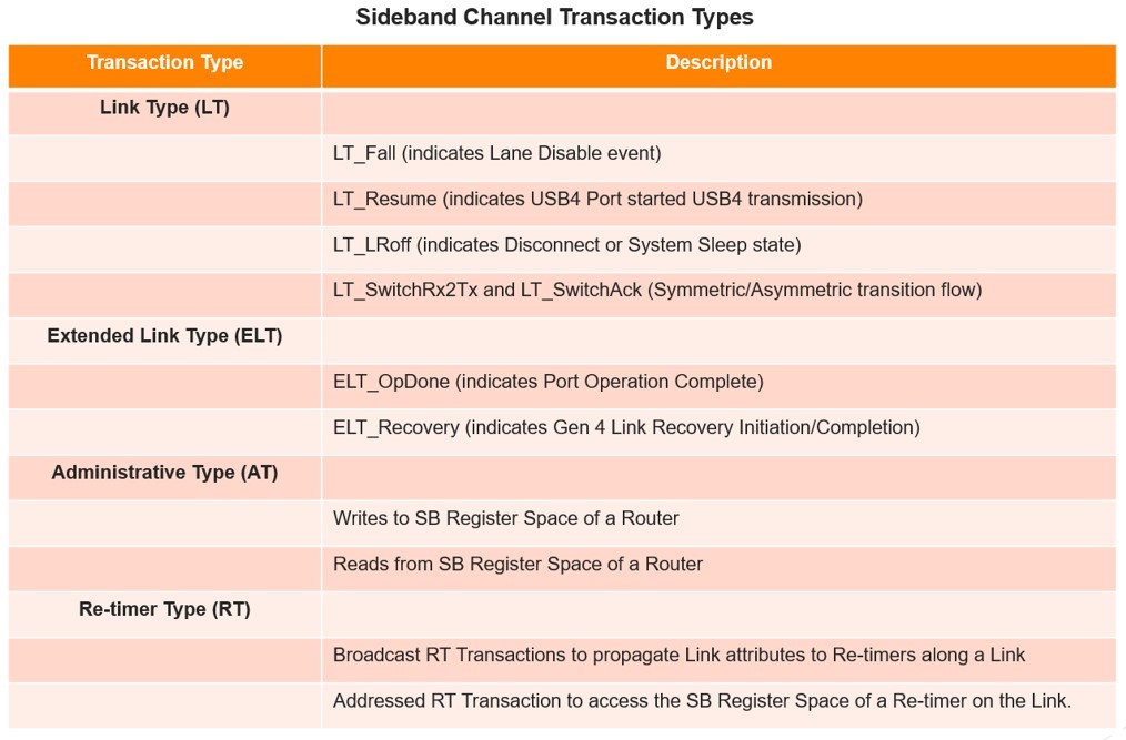
The sideband channel is a simple two-wire low-speed link operating at 1Mbps using 10-bit start/stop encoding that does not require any synchronization of its own. It supports different transaction types, namely, Link Type (LT), Administrative Type (AT), and Re-timer Type (RT), each having their specific roles mentioned in the table below.
Image may be NSFW. Clik here to view.
The sideband channel role starts from the very beginning of bringing-up of a USB4 High-Speed link through various phases of lane initialization, to link establishment, handling different aspects of link management like Sleep entry, Disconnect/Re-connect, and to supporting link recovery when the link becomes unreliable for operation.
During lane initialization phases, its functionality ranges from being a medium for router detection by way of SBTX line being made logic high by the router in phase 2, to helping each router in getting USB4 port characteristics information of its link partner in phase 3, to broadcasting the negotiated USB4 port parameters and starting High-Speed Tx and Rx traffic in phase 4, and to negotiating transmitter Feed-Forward Equalization (TxFFE) parameters between each router or re-timer and a router or re-timer adjacent to it in phase 5.
In phase 3, the USB4 port characteristics that are exchanged determine the nature of the USB4 link. These characteristics indicate bonding support, lane speed (Gen 4, Gen 3, or Gen 2), RS-FEC enabled, and asymmetric link support (3Tx, 3Rx, or only symmetric link support).
During phase 4, a USB4 port sets the lane speed and starts transmission. Routers send broadcast RT transactions to each other bearing the negotiated link characteristics. Once these transactions are complete, routers activate the transmitter on each enabled lane at the selected speed and send SLOS1 on the high-speed link. For a Gen 3 or Gen 2 link, a router indicates this start of transmission to the link partner by sending an LT_Resume transaction and setting Tx active bit in the TxFFE register of sideband register space. For a Gen 4 link, a router transmits LFPS after setting the start TxFFE bit in the SB register space of the link partner to indicate that TxFFE negotiation process can start. After LFPS is stopped, back-to-back Gen4 TS1 with the indication field set to 1h are transmitted.
At the end of phase 4, the transmitters and receivers are ready to go to phase 5, where transmitter Feed-Forward Equalization (TxFFE) parameters between each link partner are negotiated. On completion of phase 5, the high-speed link is ready to send and receive traffic and proceed with high-speed link training.
While all sideband transaction types support the lane initialization processes in various phases, link type transactions have an important role to play once the USB4 high-speed link becomes active.
LT transactions are also used to signal a change in the lane adapter state due to events such as a lane disconnect or lane disable. They are also used for communicating sleep events from a USB4 port in a router to a USB4 port on the other router.
The Gen 4 link transitions from symmetric to asymmetric and vice-versa between two routers get requested and acknowledged using LT_SwitchRx2Tx and LT_SwitchAck link type transactions, respectively.
The Gen 4 link recovery uses ELT_Recovery extended link type transaction to initiate and complete the link recovery.
The sideband channel for a TBT3-Compatible USB4 port should also honor the variations that it has for TBT3-compatibility. This includes support for the bidirectional sideband channel.
From a functionality perspective, the sideband channel may look simple. However, it has a very wide scope and a broad impact on USB4 functioning. It is, in essence, a system that contributes significantly to the smooth running of High-Speed USB4 Link.
Hence, verifying high-speed USB4 functionalities in combination with the sideband channel cannot be overlooked. It is an important verification planning advice that qualifying a USB4 design with the sideband channel functionality should never be underestimated.
To save on simulation run time for high-speed link verification, an approach that is usually taken is to bypass the sideband channel processes if the design under verification supports it and focus only on high-speed link protocol traffic. However, it does not in any way reduce the importance of verifying the high-speed link with the sideband channel processes enabled before the closure of the verification cycle, as the sideband channel is responsible for establishing, maintaining, and providing a recovery mechanism in a USB4 port.
Cadence has a mature Verification IP solution for the verification of various aspects of USB4 version 2.0 and version 1.0 design, with verification capabilities provided to do a comprehensive verification of these.
Cadence is well-known for supporting PCIe technology and providing a robust ecosystem. The PCI-SIG Developers Conference India 2024 was designed as a two-day event held in Bengaluru on November 11th and 12th, 2024. Cadence is involved in various aspects of the PCI-SIG Developers Conference, including being part of the sponsor team. Cadence set up a booth to represent work on PCIe Gen 7.
Image may be NSFW. Clik here to view.
Cadence Booth Demonstrations in PCI-SIG
Hardware demonstration of the feasibility of PCIe 7.0 physical layer speed of PMA-128Gbps in collaboration with Keysight Technologies
PCIe 7.0 VIP example demonstration using a VIP back-to-back environment
Paper presentation on effective PCIe 6.0 switch performance verification
Paper presentation on the challenges of partial header encryption in PCIe 6.0 in collaboration with Google
PCIe 7.0 Physical Layer Hardware Demonstration
The hardware demonstrates the capability of providing advanced solutions for PCIe Gen 7 to prove that our 5nm technology bird Sparrow C2 can operate at a 128Gbps data rate and give promising results with respect to both the transmitter and receiver.
The transmitter setup involved a direct connection to the scope using a test fixture of 6in MXPM and the PCB traces, which were de-embedded. Thus, only a transmitter package loss of 3dB was considered in the path.
Using the bessel filter with a bandwidth of 64GHz and transmitting a PRBS9 pattern at a data rate of 128Gbps from our Sparrow C2 test chip to the Keysight UXR Series Scope, which acted as the receiver for our transmitter, we successfully showed the signal at 128Gbps with a wide open PAM4 EYE diagram.
The receiver end includes calibration of the BERT swing to 800mV and a channel of 28dB loss added as the path from the BERT to the test chip receiver bump. To represent the worst-case ISI scenario, transmitted a PRBS31 pattern to the receiver and monitored the real time BER of ~3e-8.
Image may be NSFW. Clik here to view.
Image may be NSFW. Clik here to view.
PCIe 7.0 VIP Back-to-Back Environment
In the demo, the configuration of PCIe VIP is done to support 7.0 in serial PAM4 mode using PureView tool. Sample testbench files can be picked from the VIPCAT deliverable example. During the execution of the sanity testcase, memory transactions are initiated by RC VIP after the Gen 7 linkup. After reading from the same memory location where the write has happened, the correctness is checked to verify the functionality.
After execution, output log files are analyzed for LTSSM states, link width, PCIe capabilities, packets in packet tracker file, and waveform analysis using Verisium Debug tool. All the tools demonstrated are very effective during debugging.
The demo shows the PCIe testbench environment to test the DUT. Here, PCIe Gen 7.0 VIP is connected back-to-back, and any VIP can be replaced with user DUT.
The "Effective PCIe 6.0 Switch Performance Verification" paper was presented by Deep Mehta and co-authored by Sangeeta Soni from the VIP Product Engineering team.
Cadence discussed the performance verification of PCIe 6.0 switches. The paper highlighted the importance of performance testing in uncovering corner-case bugs and demonstrated a traffic modeling approach that can identify these issues.
Additionally, the presentation discussed latency monitoring techniques using performance measurement utilities like Performance Banner and provided implementation guidelines. Suggested findings and methodologies have value beyond IP verification, extending to pre-silicon emulation and post-silicon validation.
This paper is presented by Ritesh Mehta from Google Cloud team, co-authored by Sagar Shah, Google, and Sangeeta Soni, Cadence Product Engineering team. It highlights the challenges of Partial Header Encryption (PHE) in PCIe 6.0. It began by providing a basic overview of IDE packet structure along with an explanation of what PHE is and why it is necessary. It also covers the mechanism to reduce exposure to side-band attacks. The paper also explores the different PHE modes and finally delves into the challenges of verifying PHE, including 64B address, PH enable, and MAC calculation.
DisplayPort uses Secondary Data Packets (SDPs), which are transported over the Main-Link that are not main video stream data. This allows it to carry audio and video simultaneously. The VIP supports audio transmission both in the original mode as defined in the specification as well as just as any other SDP being transmitted.
Background of Audio Stream in DP
An audio stream is composed of the following components:
Audio_Stream SDPs
Audio_TimeStamp SDPs
Audio INFOFRAME SDPs
Partial audio time stamps within VB-ID
An Audio_Stream SDP includes the audio stream itself and some attribute information such as audio coding type and channel count. Depending on the coding type of Audio_Stream SDP, it may contain status information about the parameters of the audio stream.
Image may be NSFW. Clik here to view.
Audio_Stream SDP over Main-Link for 8-Channel Layout Audio
An Audio INFOFRAME SDP is used for transferring audio stream attributes in a separate packet. Depending on the Audio_Stream SDP’s coding type, there is some overlap between the information carried by Audio_Stream SDP and that carried by Audio INFOFRAME SDP. Whenever there is an overlap, the information carried by the Audio_Stream SDP takes precedence.
An Audio_TimeStamp SDP is used for audio clock regeneration to restore the audio Primary clock frequency that is needed for further audio processing.
An Audio_TimeStamp SDP and Audio INFOFRAME (non-Basic Audio) SDP shall be transmitted once per frame and should be transmitted during the main video stream’s vertical blanking period. Audio_Stream SDPs shall be transmitted during the main video stream’s horizontal and/or vertical blanking periods.
Additional signals, such as “the audio mute” signal for disabling audio, are carried in the VB-ID byte transmitted next to each BS control link symbol.
An audio stream is a continuous (i.e., isochronous) stream of audio samples, each of which may contain several channels of audio signals at a pre-defined sample frequency (Fs). The sample frequency is typically within the range of 32 to 192 kHz for L-PCM Audio, L-PCM 3D audio, and non-HBR compressed audio. The sample frequency of HBR audio is within the range of 256 to 1,536 kHz. The sample frequency of One Bit and DST audio is within the range of 2,048 to 24,576 kHz.
Image may be NSFW. Clik here to view.
Audio_Stream SDPs Transfer with No Video or During Video VBlank Period
Image may be NSFW. Clik here to view.
Audio_Stream SDPs Transfer with Video During Video VActive Period
Audio Frame Format
A frame is uniquely composed of two sub-frames. In 2-channel operation mode, the samples taken from both channels are transmitted by time multiplexing in consecutive sub-frames. The first sub-frame (left or “A” channel in stereophonic operation and primary channel in monophonic operation) normally starts with preamble “M”. However, the preamble changes to preamble “B” once every 192 frames to identify the start of the block structure used to organize the channel status information. The second sub-frame (right or “B” channel in stereophonic operation and secondary channel in monophonic operation) always starts with preamble “W”.
Image may be NSFW. Clik here to view.
Frame Format
Audio Format Change
The DPTX should start transmitting an audio mute signal prior to the audio format change by setting the AudioMute_Flag bit in the VB-ID. An audio format change is caused by a change in any of the following:
Between the compressed and non-compressed audio
Between different coding types
In the sampling rate
In the number of channels
Audio_Stream SDP Structure
The audio stream payload data structure has seven configurations:
or 2-channel L-PCM Audio
to 8-channel L-PCM Audio
or 2-channel One Bit audio
to 8-channel One Bit audio
to 16-channel L-PCM 3D Audio
17- to 32-channel L-PCM 3D Audio
DST audio
Speaker Mapping
Byte 4 of the Audio INFOFRAME SDP, as defined in CEA-861-F, contains information that describes the mapping of speaker locations into the audio transport channels. Image may be NSFW. Clik here to view.Image may be NSFW. Clik here to view.
Speaker Placement
Channel-to-Speaker Mapping
Channel position in the DP stream with more than two channels should exactly correspond to CTA-861. This means that gaps between channels can be present.
Image may be NSFW. Clik here to view.
Channel-to-Speaker Mapping of 3-Channel L-PCM Audio
Audio Stream Verification Challenges and Solutions
The different audio types supported by DP present several challenges.
At the transmit side, the user needs to provide the header bytes, data bytes and the AudioChannels array. VIP will internally handle:
Packing of the audio data bytes into the corresponding channels
Padding of zeroes for unused channels
Setting the various status bits in byte 4 of each channel
At the receive side, VIP has several checks to ensure that the decoded SDPs are as expected.
Decodes and validates the status bits based on the complex rules defined in the DP standard, IEC 60958 and CTA 861-F standards
Uses the frequency derived from Audio TimeStamp SDP to validate if the expected number of audio frames are received.
Summary
Cadence VIP Display Port supports the transmission and reception of the various audio coding types defined above. It also supports the entire range of channel count. Validates if the audio stream packets are transmitted at the desired frequency based on the audio sampling rate defined in the associated AudioTimeStamp SDP.
More Information
Cadence has a very mature Verification IP solution. Verification over many different configurations can be used with DisplayPort 2.1 and DisplayPort 1.4 designs, so you can choose the best version for your specific needs. The DisplayPort VIP provides a full-stack solution for Sink and Source devices with a comprehensive coverage model, protocol checkers, and an extensive test suite.
Universal Serial Bus (USB) technology is the most popular connector in every computing device, but when it comes to embedded applications, where only a specific device function may be required, the architectural philosophy of the USB technology becomes inefficient.
One example could be USB cameras. With increasing user expectations of camera resolution and frame rates, the bandwidth constraints of USB 2.0 require today’s cameras to aggressively apply compression to fit within its bandwidth limitations. Even with compression, next-generation cameras will exceed the USB 2.0 bandwidth limitations.
If USB 3.x technology is used to address the bandwidth need, it is not an optimal solution for these camera devices because it is a symmetrical link offering the same bandwidth capacity to both downstream and upstream traffic. For a camera device, the bandwidth requirement is asymmetrical. A USB 3.x camera is not an optimal solution for embedded applications and is also not cost-effective as compared to USB2 devices.
This usage model reveals a technology gap in the platform I/O space, yielding an inflection point of opportunity. The eUSB2 Version 2.0 (eUSB2V2) is developed to deliver a scalable I/O technology specifically designed for inside-the-box (embedded) USB applications, optimizing for performance, power, and cost. It supports a low-voltage, power-efficient PHY with gigabit rates on a USB 2.0 architectural framework, i.e., half-duplex link and transactional protocol.
Topology
The eUSB2V2 is primarily a performance enhancement to eUSB2 native mode to provide more bandwidth for peripherals, such as embedded cameras, by adding significantly higher data rates to USB 2.0 while maintaining a low-voltage electrical interface. As eUSB2V2 is intended to support in-box applications in native mode, the physical channel is relatively simple, with both the host and the peripheral being inside the system’s physical boundary. An external cable or connector is not supported; however, one re-driver between the host and peripheral is allowed.
Image may be NSFW. Clik here to view.
Key eUSB2v2 PHY Features
eUSB2V2 transfer rates:
HSSx-speed: Symmetric operation where the link is operating at 960Mbps to 4.8 Gbps in both transfer directions
Optionally, if symmetric 480Mb/s operation is desired, it shall be done via eUSB2 native mode
HSUx-speed: Asymmetric operation where the link is operating at 960 Mbps to 4.8 Gbps in the upstream direction and at 480 Mbps in the downstream direction
HSDx-speed: Asymmetric operation where the link is operating at 960 Mbps to 4.8 Gbps in the downstream direction and at 480 Mbps in the upstream direction
Reduced bus turnaround time:
Only in-box applications are supported, minimizing peripheral interconnect propagation times.
Enables shorter interpacket delays
Increased maximum size of bulk packets from 512B to 1024B
Enables more efficient isochronous transfers to improve transaction efficiency:
More than 3072B of Isochronous packets may be transferred per service interval (SI)
Burst transactions are enabled for isochronous transfers, allowing the transmission of up to three data packets after a single IN or OUT token, thereby reducing the bandwidth requirement to n/3
If more than 1024B of isochronous data is transferred per microframe, then all data packets must be 1024B, with the remainder in the last packet
Supports link power management LPM-L1 (L1) and Suspend (L2)
eUSB2v2 implementation is based on UTMI 2.0 Parallel Mode
Supports register access protocol (RAP) for eUSB2V2 peripheral or re-driver configurations
Fully compatible with USB 2.0 base spec at the protocol layer
No change to the USB 2.0 software programming model
Not compatible with the physical layer defined by USB 2.0 or eUSB2
Not compatible with standard USB 2.0 connectors defined by USB 2.0 and its derivatives
Cadence has a comprehensive Verification IP solution for the verification of various aspects of eUSB2 Version 2.0 (eUSB2v2), with capabilities provided to do a comprehensive verification of all features. You may write to support@cadence.com or contact a local Cadence representative to get more details on eUSB2v2 VIP.
With the arrival of Flit Mode, the information hold by the TLP header was reorganized. In addition to the base header, Orthogonal Header Content (OHC) may be added into the TLP. OHC works as an extra header for the TLP, incorporating information fields that are needed depending on the TLP type.
Background of OHC
There are multiple OHC types. Each one includes a specific set of information in the TLP packet. For specific TLP types, a specific OHC content must be included by the Transmitter.
It is permitted to include any combination of OHC content in the TLP's Header. When present, OHC must follow the Header Base in A-B-C-E order. The number of included OHC and types is indicated by the OHC field in the first DW of the TLP Header. A TLP Header may include up to 7 OHC.
Image may be NSFW. Clik here to view.
The OHC[4:0] field indicates the presence of "Orthogonal Header Content" (OHC) encoded as:
0 0000b = No OHC present
x xxx1b = OHC-A present
x xx1xb = OHC-B present
x x1xxb = OHC-C present
0 0xxxb = No OHC-E present
0 1xxxb = OHC-E1 present
1 0xxxb = OHC-E2 present
1 1xxxb = OHC-E4 present
OHC Types – When to Use
OHC-A1
OHC-A1 must be included for Requests that require any of the fields included in OHC-A1.
Memory Requests with explicit Byte Enables and/or PASID Address Routed Messages with PASID and Route to Root Complex Messages with PASID Translation Requests.
For all Memory Requests, it is permitted for OHC-A1 (see Figure 2-7) to be present. For Memory Requests, when OHC-A1 is not present, the value of the Last DW Byte Enable field must be treated as 1111b for Requests with Length greater than or equal to 2 DW, and the value of the 1st DW Byte Enable field must be treated as 1111b. If a Request requires Byte Enables field values other than these, then OHC-A1 must be present. When OHC-A1 is present, the PASID, PMR, and ER fields are valid if and only if the PV bit is set.
Image may be NSFW. Clik here to view.
OHC-A2
OHC-A2 must be included for all I/O Requests.
Image may be NSFW. Clik here to view.
OHC-A3
OHC-A3 must be included for all Configuration Requests.
Image may be NSFW. Clik here to view.
OHC-A4
OHC-A4 must be included in ID Routed Messages when Destination Segment or PASID is required.
Image may be NSFW. Clik here to view.
OHC-A
OHC-A5 is required for Unsuccessful Completions, Non-UIO Completions with Lower Address[1:0] not equal to 00b, and Completions that require the Destination Segment due to the associated Non-Posted Request containing a Requester Segment that does not match the Completer's captured Segment.
When OHC-A5 is not present, it is implied that the Completion Status is Successful, that Completer Segment and Destination Segment need not be explicitly indicated, and that, for non-UIO Completions, the Lower Address[1:0] = 00b.
Image may be NSFW. Clik here to view.
OHC-B
When TLP Processing Hints (TPH) are used, OHC-B must be included with the appropriate PH and ST values.
Image may be NSFW. Clik here to view.
OHC-C
IDE TLPs must include OHC-C. Non-IDE Request TLPs must, in some cases, also include OHC-C to indicate the Requester Segment.
Image may be NSFW. Clik here to view.
OHC-E
The information previously present in the End-to-End Prefix is now incorporated in the TLP's header as OHC-E. OHC-E conveys content that would otherwise use E-E Prefixes 0011 to 1111.
Image may be NSFW. Clik here to view.
Image may be NSFW. Clik here to view.
Image may be NSFW. Clik here to view.
OHC Verification Challenges and Solutions
The OHC brings new rules for the TLP header organization. The TLP header size changes according to the number of included OHC instead of relying only on the TLP type. Some features now require specific OHC, like Integrity and Data Encryption (IDE) and Process Address Space ID (PASID). End-to-end prefixes can be easily detected at the end of the header.
The solution naturally requires verification to check when OHC are included, violating the rules that allow their use. The contents inside the OHC fields need to be checked as the fields on the base TLP header. Implementers need to know all the OHC that may be included in the TLP packets and be fully aware of all the rules that define when each one must be used.
Different RTL designs often require different specially designed parallel interfaces. These different interface requirements serve varying needs, such as certain blocks not being ready when the design is under development. To speed up simulation during unit testing, DisplayPort needs to connect to other protocols. Instead of creating a new physical pin interface, this blog introduces a Transaction-Based Customer Interface, which is compatible with all users' specific parallel interface requirements. The traditional way of creating a new physical pin interface is time-consuming. Even a slight difference in the interface definition requires the development of a full pin interface as the pin interface is 1 to 1 solution. Also, multiple physical interfaces are confusing to the user. This interface allows users to use the VIP transactions and callback instead of predefined physical pins. For example, customers request a 32-bit aligned interface and CIO mode interface. With traditional methods, VIP needs to create two different parallel interfaces. With the transaction-based customer interface, VIP only uses one interface to fulfill two different customer requirements.
Solution
To address the above issue, we are proposing the Transaction-Based Customized Interface is a configurable interface compatible with all user's specific parallel interface requirements. This interface allows users to use the VIP transactions and callback instead of predefined physical pins. Instead of using the signals on physical pins, the DisplayPort VIP provides callbacks and transactions. Users can use callbacks and transactions to access the data and modify a transaction inside of VIP. This provides flexibility to the user.
Below is the test topology of Source VIP connecting to Sink DUT without the pin interface. Figure 1 shows the flow with Source as VIP and Sink as DUT. In this scenario, Source VIP provides data in the form of predefined field transactions through callback. The predefined fields data masks or bundles to form a customer-defined pin interface in the testbench. Special sideband signals are also extracted from transaction fields. DUT detects the data and control signals through the defined pin interface.
Image may be NSFW. Clik here to view.
Figure 1: Source VIP connects to Sink DUT with the Transaction-Based Customized Interface
Example
Interface#1 – 32-bit Parallel Interface
In 128b/132b channel coding, the customer requested a 32-bit parallel interface instead of transmitting/receiving 1 bit at a time in order to fasten simulation time without a serialization block. From the spec, each block has 132bit (FEC disabled) or 129bit (FEC enabled). This nature block is not aligned with the 32-bit requirement. Blocks need to break to 32 bits. Traditionally, VIP must create a new physical interface, serialize the block first, and reform it to align as 32-bit symbols. In the proposed way, VIP provides the transaction, and TB aligns it to a 32-bit symbol, and there is no need to create a physical interface. Below is the figure to illustrate that VIP is able to provide 32-bit data from a transaction-based interface.
Image may be NSFW. Clik here to view.
Figure 2: Customized 32bits parallel interface
Interface#2
Another interface is designed with a Transaction-Based interface. The testbench is able to extract from transactions and fields to generate data and control signals as they request.
Image may be NSFW. Clik here to view.Figure 3: Customized CIO interface
Conclusion
The DisplayPort VIP Transaction-Based interface supports both 128b/132b channel coding and 8b/10b channel coding, with different features, such as ALPM (Advanced Link Power Management) and FEC (Forward Error Correction). User can verify their RTL designs with different interfaces using a Transaction-Based interface. In 128b/132b channel coding, the user can configure a symbol-based 32-bit interface, or super symbol-based 132-bit, etc. In 8b/10b channel coding, the user can configure to include or not include skew, FEC, etc. Users can also configure it to switch between the 8b/10b channel and the 128b/132bit channel.
This Transaction-Based customer interface can support all customers' specific parallel interfaces. It is compatible with all customers' specific parallel interfaces to fasten the integration and simulation time.
More Information
Cadence has a very mature Verification IP solution. Verification over many different configurations can be used with DisplayPort 2.1 and DisplayPort 1.4 designs, so you can choose the best version for your specific needs. The DisplayPort VIP provides a full-stack solution for Sink and Source devices with a comprehensive coverage model, protocol checkers, and an extensive test suite.
As technology continues to advance, so do the ways we connect and manage memory and devices in our computing systems. The latest version of Compute Express Link (CXL) 3.1 introduces a feature known as extended metadata. This feature brings significant improvements to how memory transactions are handled, leading to better performance and efficiency. Let's break down what extended metadata is, why it's important, and how it could make a difference in your systems.
What Is Extended Metadata?
Extended metadata in CXL 3.1 is basically extra information up to 32 bits that gets sent along with memory transactions. CXL Expansion memory to have the ability to receive and transmit additional information for a given cache line. The device stores the additional Extended Meta Data field for a given cache line. This added data provides more context about what's happening during these transactions, helping systems manage memory and devices more effectively. Think of it as extra details that help the system make smarter decisions about how to handle data.
Why Does Extended Metadata Matter?
Better Transaction Handling: Extended metadata allows systems to include detailed information about each memory transaction. This could be details like what type of transaction it is or how important it is. With this extra information, systems can better understand and manage each transaction, which can reduce delays and improve overall performance. For example, if a transaction needs to be processed quickly, it can be flagged with extended metadata, So the system knows how to prioritize it. This helps ensure that critical tasks are handled promptly, leading to a smoother operation.
Improved Quality of Service (QoS): In computing, managing different types of data traffic efficiently is crucial. Extended metadata helps by providing information that allows systems to prioritize and manage traffic more effectively. This is especially important in environments where multiple tasks or applications are competing for the same resources. By using extended metadata, CXL 3.1 helps balance the load, ensuring that important tasks get the attention they need, and that resources are used in the most efficient way possible.
Data Tagging: When things go wrong in a system, understanding what happens can be tricky. Extended metadata helps by giving more detailed information about errors and system issues. This makes it easier to figure out what went wrong and how to fix it quickly. For example, if a memory transaction fails, extended metadata can provide insights into why it failed, helping you address the problem faster and keep the system running smoothly.
How Does this Affect Real-World Applications?
The benefits of extended metadata have practical implications across various fields:
Data Centers and Cloud Services: These environments rely on efficient management of resources. Extended metadata helps by improving traffic management and ensuring resources are used effectively.
High-Performance Computing (HPC): In HPC, where performance is critical, the enhanced error reporting and transaction handling provided by extended metadata can significantly boost reliability and efficiency.
Artificial Intelligence (AI) and Machine Learning (ML): For AI and ML applications, which often deal with large amounts of data, flexible memory management and improved performance are key advantages.
Verification Challenges and Solutions
Verifying that the EMD carries the correct metadata and that it is interpreted properly at the receiving end. Use randomized testing to uncover corner cases in EMD encoding and decoding.
Validating the correct integration of EMD within the S2mDrs Trailer Slot, especially when multiple slots are used in a single link layer flit. Use boundary condition tests to verify correct handling of partial, truncated or malformed flit.
Ensuring that systems and devices without EMD support still function correctly and ignore EMD processing and report error for same. Use configuration option to disable EMD in testing and verify that device operate without issues.
Conclusion
Extended metadata in CXL 3.1 is a significant advancement that brings extra detail and control to memory transactions. This feature makes it easier for systems to handle complex tasks and manage resources effectively. As computing needs continue to grow, understanding and utilizing features like extended metadata will be crucial in keeping systems running at their best.
The AMBA LTI (Local Translation Interface) defines the point-to-point protocol between an I/O device and the TLBU (Translation Buffer Unit) of an Arm System Memory Management (SMMU). The LTI protocol is used by systems built based on the Arm System SMMUv3 architecture specification.
The LTI protocol defines three different channels to request a translation for each transaction coming from an I/O Device. Additionally, it defines interface management signals and credit signals for flow control. LA and LR channels can have multiple virtual channels, which enable one VC to progress when another is blocked to avoid deadlock scenarios and can result in higher bandwidth.
LTI Channel
The LTI interface contains the following channels:
LA Request channel: Address and attributes that require translation are sent to the TBU.
LR Response channel: Provides the translated address and attributes to the LTI device.
LC Completion channel: LTI devices must provide information about completion to the TBU.
As shown in the following image, the LTI Manager sends the request on the LA channel for each transaction from the device, which requires a translated address. LTI-TBU component passes the translated address and response on the LR channel. LTI enables devices to directly request a translation for each transaction while leaving the TBU to manage the Translation Lookaside Buffer (TLB). If LTI-TBU does not have a translated address, it sends a request to the TCU component using DTI protocol and forwards the translated address to the LTI Manager. For each translation response, the LTI Manager sends a completion message using the LC channel.
Image may be NSFW. Clik here to view.
LTI Transaction Flow
A complete LTI transaction consists of a message on all three channels as shown below figure.
The manager sends a request to the LA channel.
The subordinate sends a response on the LR channel, enabling the translated transaction to be issued downstream.
The manager sends a completion on the LC channel, once the downstream transaction is complete.
The following diagram represents the timing for the transactions initiated from device flows through the system.
Image may be NSFW. Clik here to view.
Cadence AMBA LTI VIP provides complete solutions with Active Drive and Passive Agent with exhaustive protocol checks, functional coverage, and building block sequences to implement complex test cases. The following image represents back-to-back VIP communication where each Active VIP component can be replaced with RTL for verification.
Image may be NSFW. Clik here to view.
LTI Verification IP provides different levels of callbacks for score boarding and erroneous scenarios.
More Information
Cadence provided complete Verification IP solution for unit level to SoC level Verification.
To get more details on Cadence Simulation Verification IP, please visit our website Cadence Simulation VIPor simply reach out to discuss with Cadence Verification IP experts.
USB Promoter Group has released the eUSB2® Version 2.0 specification (eUSB2v2) in August 2024, which is developed to deliver a scalable I/O technology, specifically designed for inside-the-box (embedded) USB applications, optimizing for performance, power, and cost.
As per the new specification, eUSB2v2 compliant designs will support up to 4.8Gbps bandwidth in both directions when operating in symmetric operation. When operating in asymmetric operation, designs will support 960Mbps to 4.8Gbps in the upstream/downstream direction and at 480Mbps in the downstream/upstream direction.
Key features included in eUSB2v2 specification:
Increased bandwidth up to 4.8Gbps
Symmetric operation, up to 4.8Gbps in both directions
Asymmetric operation, 960Mbps to 4.8Gbps in the upstream/downstream direction and at 480Mbps in the downstream/upstream direction
Support of only in-box applications for lower bus turnaround time
Increased maximum size of bulk packets
Cadence announces the industry's first Verification IP for eUSB2v2 Specification compliant designs. It supports Host and Device modes. For more details, refer to the Cadence eUSB2v2 VIP page or send an email to support@cadence.com or contact your local Cadence representative for more details on eUSB2v2 VIP.
As we welcome 2025, let’s take a moment to reflect on the most viewed blogs and videos of the past year and review the developments in education throughout 2024.
We would like to extend our gratitude to all our colleagues who regularly share blogs featuring the latest and most engaging teaching and learning materials. Here are the links to some of the most viewed blogs/ training byte videos/webinars/RAK:
We would also like to invite our customers to one of our Cadence offices for a"live training" with one of our experienced engineers. We also arrange an offsite or "Blended" training for you.
And here is some more interesting news from 2024
The Cadence Design System training team has introduced an online option called "Accelerated Learning" designed to help you effectively learn Cadence Technical Solutions and Products. Before starting an accelerated online course, you can take a pre-quiz to assess your current knowledge, skip familiar content, and achieve your training goals more quickly. This blog post provides further guidance and explanations.
The accelerated learning option is currently available for the following System Design and Verification online training courses, with more to come:
We are proud to announce the development and release of our Onboarding Curriculum specifically for new hires, allowing them to quickly learn the tools and technologies necessary for productivity. You can read more about it in this blog.
Additionally, we have released our Digital Design and Verification Academic Curriculum, which includes materials for a 15-week course and links to Cadence® courses featuring hands-on labs. Educators have the flexibility to choose which lectures to teach based on their goals. This curriculum aims to prepare undergraduate students for roles as Digital Design Engineers or Front-end Verification Engineers. It covers digital design concepts, Verilog, and verification technologies, and introduces SystemVerilog and UVM.
All customers with a valid Cadence ASK account can access the training online 24/7 at no cost. To learn more about maximizing your experience with the Cadence ASK portal, check out these blog posts:
For any questions, general feedback, or even if you want to suggest a future blog topic please leave a comment in the Cadence Community Forum. You can also subscribe to the blog series to stay up to date about new trainings and training videos available at our new designed Cadence Training site.
Do send your response to the three questions in the below image to eur_training@cadence.com. Your feedback is valuable to us!
We all agree that time is precious. As PSS (Portable Stimuli Standard) models get larger, the time it takes for the whole model to be loaded in Cadence Perspec Composer might become meaningful. In this blog, we will look into two practices that help ...(read more)Image may be NSFW. Clik here to view.
Designs are tested in the labs for various electrical compliance tests defined in the electrical compliance test specifications before getting certified. There are defined processes and steps that a design must go through for such testing. Such tests are focused tests and need complete control of the specific parts of the design to do targeted testing with the generated stimulus. Hence, they are done outside of the normal protocol flow by bringing the specific part of a design under test in a defined condition and getting it ready. To do so, protocol specifications define compliance operations.
Even though these compliance tests are mostly electrical in nature, the design under test still needs to go through defined logical steps to get the specific part ready for the test, to provide the stimulus, and to measure the effect of that stimulus.
USB4, too, has defined compliance port operations. These port operations are used to bring transmitters and receivers of a design under test into compliance mode and to execute tests like bit error tests, burst error rate tests, clock switch tests, TxFFE equalization tests, electrical Idle tests, etc.
Various compliance port operations and their respective intents are listed in the table below,
Image may be NSFW. Clik here to view.
The SET_TX_COMPLIANCE port operation provides the flexibility to have a USB4 Port transmit the various possible patterns that are required for the transmitter compliance testing. These patterns encompass Gen2, Gen3, and Gen4 link speeds. For Gen2/Gen3, they are PRBS31, PRBS15, PRBS9, PRBS7, SQ2, SQ4, SQ32, SQ128, SLOS1. For Gen4, they are PRBS11, PRTS7, PRTS19, STAIRS112, SQ224. The applicability of when to use which pattern depends on the test defined in the electrical compliance test specification. It varies according to the test objectives.
The SET_RX_COMPLIANCE port operation puts a receiver to the compliance test. It provides the option to indicate to the receiver whether the transmitter is transmitting PAM2 or PAM3 encoded data. The transmitter knows when to switch the transmitting pattern through the completion data of this port operation at the receiver. This completion data indicates whether the receiver is ready for PAM3 and SSC activation.
The LFPS_TEST port operation is used to test the transmitter and receiver of LFPS signaling. It provides various modes for LFPS transmission, i.e., to transmit 100 cycles of LFPS, transition to electrical idle for tPreData, and start sending SLOS1 (for Gen2 or Gen3) or PRBS11 (for Gen4). Such modes help test the LFPS scenarios that are part of the protocol flow.
The port operations are applicable whether the link is symmetric or asymmetric for Gen4 link speed. For testing an asymmetric link SET_LINK_TYPE port operation is used to force the link to come up as an asymmetric link after lane initialization before using other port operations.
Compliance testing involves compliance software to test a Port Under Test (PUT). VIP has appropriate controls to mimic a PUT and functionality of compliance software.
An example flow for checking the receiver compliance of the Rx adapters of a Gen4 asymmetric link is depicted in the table below. In this, the PUT is to be tested for receiver compliance, with VIP being used to send the relevant test patterns to the adapters of the PUT.
Image may be NSFW. Clik here to view.
Image may be NSFW. Clik here to view.
In addition to the compliance port operations, there are a few service port operations as well that are required. They are ROUTER_OFFLINE_MODE to put a USB4 port in offline mode, ENUMERATE_RE-TIMERS to cause a USB4 port to send a broadcast RT transaction, and FEC_ERRORS_STAT to start, stop, and read the FEC errors counters of a port.
Before a port operation can be initiated, its metadata and data should be programmed in the relevant sideband registers. Sideband registers 8, 9, and 18 are used for this purpose, namely for writing the opcode, metadata, and data or completion data of a port operation, respectively. The type of metadata that is required is as mentioned in the table above. It influences the ways a port operation executes the intended test objectives.
Cadence has a mature verification IP solution for the verification of various aspects of USB4 version 2.0 and version 1.0 design, with verification capabilities provided to do a comprehensive verification of these.
Tcl is a versatile scripting language used in automation, testing, networking, and more. Tcl plays a crucial role in Electronic Design Automation (EDA) tools used in the VLSI industry.
Leading EDA tools rely on the TCL scripting language to automate design flows, customize tool behavior, and streamline chip design processes. TCL provides a straightforward interface for performing various tasks with EDA tools, interactively performing multiple functions with the tool.
Whether you are a VLSI engineer, ASIC/FPGA designer, or a student aspiring to enter the semiconductor industry, mastering Tcl will give you a significant edge.
This course covers the following modules:
Course overview
Tcl basics
Mathematical expressions and procedures
Control flow
Strings
Lists, arrays, and dictionaries
FileIO and program access
Regular expression
Advanced Tcl scripting
This course starts with an introduction that explains high-level information about the Tcl language, such as its features, primary applications, and usage in EDA tools.
Then, it covers the basics of the Tcl language, such as syntax, commands, variables, and the command evaluation process. This is followed by mathematical operations, procedures, and various control flows.
After that, strings, which is the basic datatype of the Tcl language, are covered, along with various string operations supported by the language.
Then, the lists, arrays, and dictionaries are explained with associated examples and operations. This is followed by the files, related operations, and Tcl processes.
Finally, regular expressions and concepts used in advanced Tcl scripting are explained.
This Tcl course is a creation from the old combined Tcl/Tk course. It has an audio transcript for self-paced learning. Stay tuned for the Tk course, which will also be released soon.
The course is available here on the Cadence ASK(formerly Cadence Learning and Support) page:
Image may be NSFW. Clik here to view.
You can also find a variety of troubleshooting videos covering a multitude of topics on Cadence ASK.
For questions and inquiries or issues with registration, reach out to us at Cadence Training.
Want to stay up to date on webinars and courses? Subscribe to Cadence Training emails. To view our complete training offerings, visit the Cadence Training website.
Verisium WaveMiner is part of the Verisium suite of AI-driven verification tools that automate the root cause analysis of misbehavior introduced between two versions of the same RTL design. By analyzing passing and failing waveforms, Verisium WaveMiner ranks and highlights the signals and timepoints relevant to the misbehavior, simplifying the regression debug process.
Why Do We Need Verisium WaveMiner?
Narrows down debug scope by ranking culprit signals
Minimizes uncertainty by engaging stakeholders quickly
Reduces regression debug effort and maximizes verification throughput
Helps to dismiss unlikely root causes and identify design changes causing failures
Verisium WaveMiner Inputs and Outputs
Inputs
One or more passing waveforms and one or more failing waveforms
Generated with two different versions of the same design
Analysis scope: Two snapshots or user-defined list of signals/instances
Outputs
Text report with ranked culprit signals and simulation time points
Visualization in Verisium Debug
Interactive navigation through ranked signals and timepoints
Verisium WaveMiner Flow
Verisium WaveMiner performs signature mining on passing and failing waveforms, cross-validates the results, and ranks the design signals and simulation timepoints according to their contribution to the misbehavior. The results are visualized in Verisium Debug for detailed analysis.
WaveMiner Functionality
Signature mining from multiple passing and failing waveforms
Ranking of failure root cause candidate signals and timepoints
Automatic invocation of Verisium Debug for detailed analysis
Minimizes debug effort and improves the quality of results (QoR)
Verisium WaveMiner Dual Waveform GUI View
Verisium WaveMiner Setup
Environment Setup
Set environment variables for Verisium Apps and Verisium Debug
Install required licenses for waveform analysis
Running Verisium WaveMiner
Use the provided commands and scripts to run Verisium WaveMiner
Generate a ranked list of signals and timepoints for debugging
Additional Resources
The below listed training bytes channel and an RAK from Cadence ASK will help you navigate through the complete Versium WaveMiner flow and features.
Verisium WaveMiner is a tool in the Verisium suite that automates the regression debug process. It performs signature mining on passing and failing waveforms, ranks design signals and simulation timepoints based on their contribution to misbehavior, and visualizes the results in Verisium Debug. By minimizing debug effort and improving the quality of results, Verisium WaveMiner is essential for designers and verification engineers.
This comprehensive guide captures the key points and functionalities of Verisium WaveMiner to aid users in leveraging its full potential.