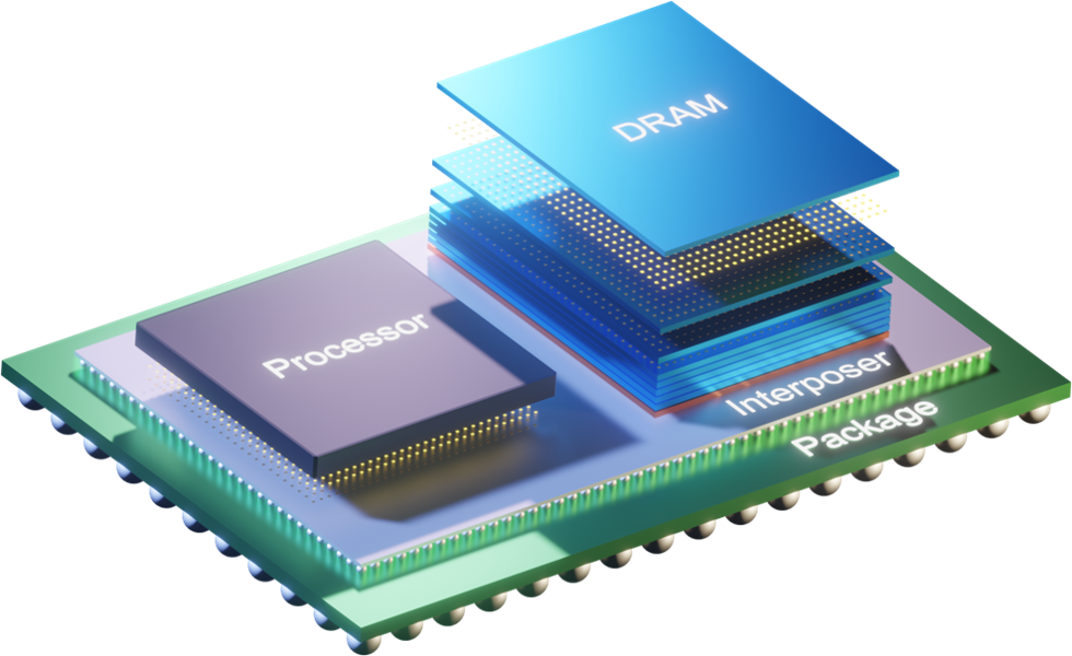
HBM is a JEDEC (Joint Electron Device Engineering Council) standard-defined DRAM (Dynamic Random Access Memory) with a 3D-stacked memory architecture that reduces power consumption and has a small form factor. Because of these unique characteristics, HBM is the leading choice for high-performance computing (HPC), graphics, networking, artificial intelligence (AI), and machine learning (ML). The differentiator with HBM memory is that it is stacked and connected to the System-on-Chip (SoC) by an interposer in the same package as referred to in the image below. This poses several challenges for the testability and validation of the DRAM.

Apart from HBM, DRAMs are individual memory components external to the package, and for them, the memory capacity expansion or replacement capability is quite normal. While HBM is tightly coupled to the chip die, and there is no way to get capacity expansion or memory replacement. If anything’s wrong with HBM, the whole SOC becomes useless. This is also a strong cause to have testing and training capabilities for HBM.
IEEE 1500 is a widely adopted testability standard that helps in testing core designs within SOC. IEEE 1500 has been an integral part of HBM DRAMs since the inception of HBM memory definition to the latest HBM3 memory. It is a serial interface, and it clocks much slower compared to HBM DRAM.
HBM DRAM supports many test instructions through IEEE 1500 to help bump connectivity testing and its repair, training, mode register setting, asynchronous reset generation, channel identification, temperature sensing, etc. HBM DRAM is a multichannel device, and to aid the parallel execution of IEEE 1500 instructions, an extension of the IEEE 1500 is used where the serial output pin WSO is defined per channel.
The test instructions and their purpose are as follows:
- Boundary Scan: Extest Tx/Rx are instructions to confirm the data connectivity. Here, data sent/received to/from the memory controller to HBM memory. IEEE 1500 instructions help to drive/read back the boundary scan data.
- Loopback mode: The feature helps to achieve signal integrity on both command and data buses. The sampled loopback data is stored and can be read back by IEEE 1500 instructions. The LFSR (Linear Feedback Shift Register) and MISR (Multiple Input Shift Register) can be used to generate patterns for the loopback data.
- Lane repair: It is also known as interconnect redundancy remapping. The soft/hard lane repair instructions remap the inputs/outputs. Remapping by soft lane repair is not preserved and can be used to confirm the repair of interconnect issues; then, hard lane repair can be performed to make the repair permanent.
- Device Information: With device ID instructions, as the name suggests, various information about HBM DRAM can be read, such as unique device id.
- Probe or Set DRAM configuration: Using the mode register dump set instruction, the current set of configuration values can be captured back. Also, by using set, newer configuration values can be set simultaneously to all the mode registers.
- Write Data Strobe (WDQS) Training: With the change in temperature and voltage on the HBM DRAM, the clock delay can shift. Using IEEE 1500 instructions, users can initiate this training and learn its status.
Cadence MMAV (Memory Model Advanced Verification) VIPs (Verification IP) for HBM, HBM2, HBM2E, and HBM3 are comprehensive VIP solutions and support all the above-listed IEEE 1500 features along with core memory functionalities and checkers. Users can configure/ read all the IEEE 1500 instruction registers via a backdoor apart from the usual protocol behavior. HBM3 is a JEDEC standard since 2022, and Cadence is actively tracking the development of the HBM standard at JEDEC.
More information on Cadence HBM3 VIP is available at the Cadence VIP Memory Models Website.
If you have any queries, feel free to contact us at talk_to_vip_expert@cadence.com